


Powering AI with atomically-thin materials
Powering AI with atomically-thin materials
Our vision
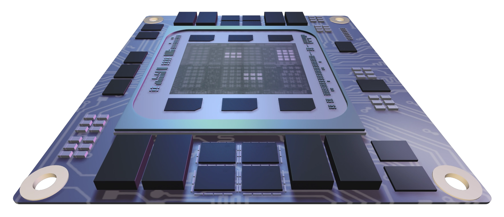
CDimension: Engineered to scale the next computing frontier
CDimension is rethinking chip design from the ground up, delivering solutions that are faster, smarter, and more compact. We’re moving beyond the limitations of traditional technology. Our foundational innovations in advanced materials and semiconductor integration unlock unprecedented gains in performance, efficiency, and scalability – ranging from 10x to 1,000x times greater than current approaches. With a powerful suite of products, CDimension is building the essential chip infrastructure for today’s and tomorrow’s computing breakthroughs.
Our technology
Advanced material synthesis
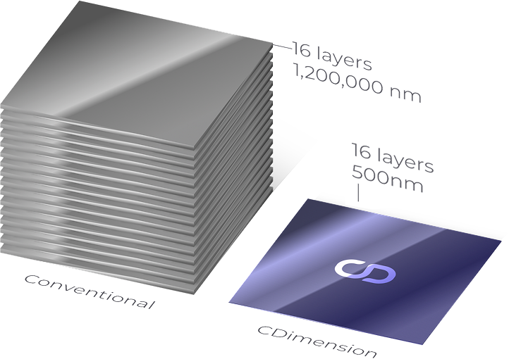
At the heart of CDimension’s innovation is a groundbreaking, low-temperature, wafer-scale process for synthesizing atomically thin semiconductor materials. This proprietary technology, initially focused on MoS₂ (molybdenum disulfide), enables the creation of atomically-thin chiplets, deposited onto silicon (Si CMOS) wafers. Crucially, our process maintains the integrity of the underlying circuitry, ensuring high-quality integration without damage.
This advanced material synthesis unlocks a host of powerful benefits:
- Dramatic performance and efficiency gains: Our atomically-thin MoS₂-based transistors can deliver up to 1000x improvements in energy efficiency compared to conventional silicon at similar scale
- Unmatched density and compactness: Higher transistor density enables the creation of devices that are both more compact and incredibly powerful
- Cost-effective innovation: By utilizing a back-end-of-line (BEOL) process, we integrate new material layers onto wafers after conventional silicon circuitry is complete, avoiding the prohibitive costs of cutting-edge lithography
- Future-proof for 3D integration: This same BEOL process is perfectly suited for seamless 3D chip integration, paving the way for the next generation of computing
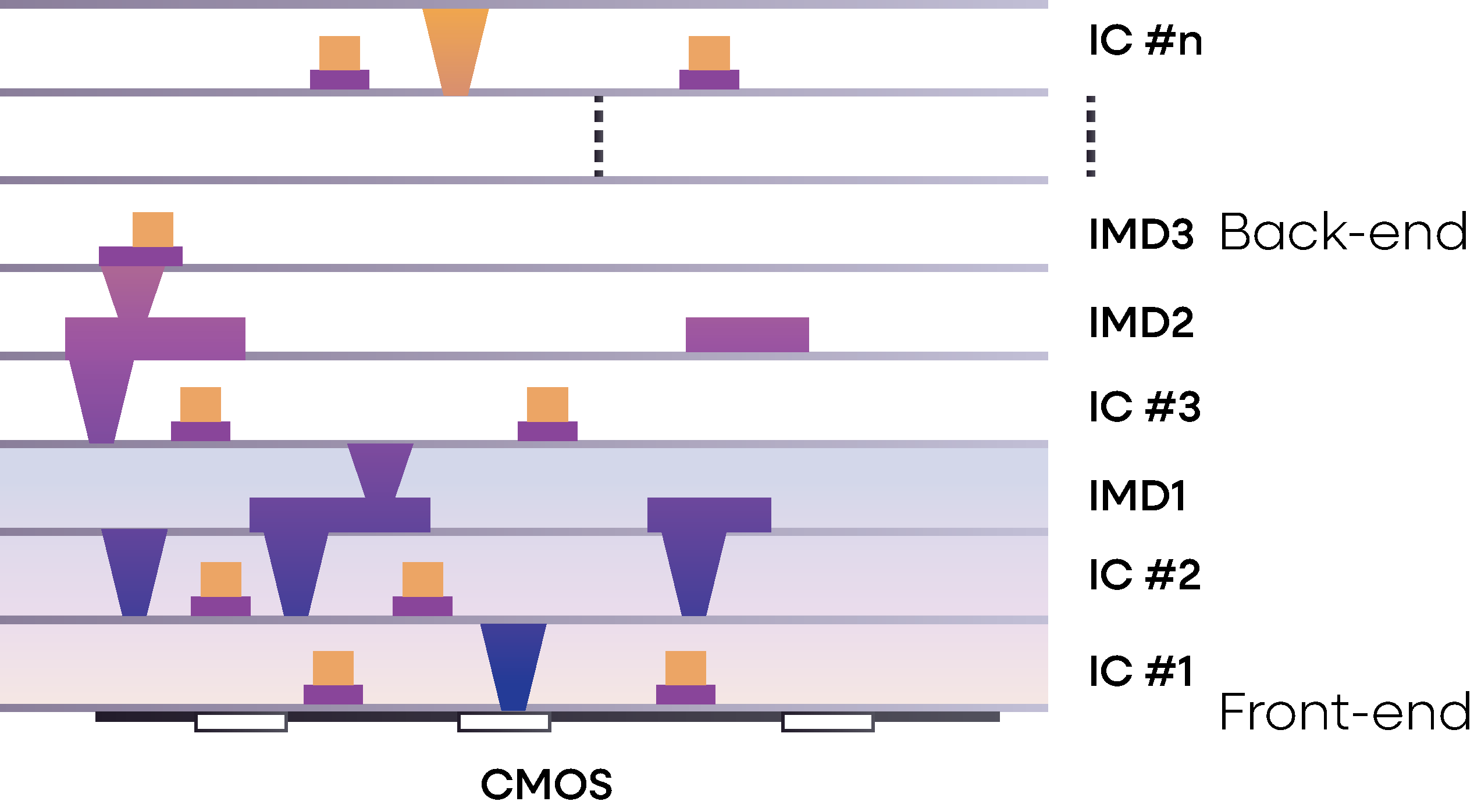
Monolithic architecture
Beyond individual components, CDimension’s monolithic architecture technology vertically integrates compute, memory, and power layers within a single unified chip. The result is a compact, unified architecture that greatly reduces interconnect distances and parasitic losses. Signal delays, such as memory walls from logic, are also greatly shortened. It all leads to systems that are faster, simpler, more efficient and more cost-effective.
This unified monolithic architecture brings a number of benefits:
- Unrivaled compactness and cost savings: Consolidating high integration into a single integrated circuit (IC) significantly reduces space requirements and lowers overall system costs
- Superior thermal control: Our design inherently improves thermal management, leading to less heat generation and radiation
- Blazing-fast data flow: Data can now flow between components at up to 1,000x faster speeds, revolutionizing processing capabilities
- Massive reduction in parasitics: We cut interconnects and parasitic losses by up to 1,000x, ensuring cleaner, more efficient signal transmission
- On-chip power efficiency: Integrating the power management integrated circuit (PMIC) directly onto the chip virtually eliminates the typical 20-30% power loss seen when the PMIC resides on a separate printed circuit board
All of this enables staggering performance upgrades
0
x
faster on-chip data links
0
x
increase in memory bandwidth and density
0
x
energy efficiency at the memory level
0
x
higher operating frequency with reduced parasitic losses
Working with us
CDimension materials available now
CDimension provides high-quality 2D materials and integration services at research-accessible cost, enabling breakthroughs in BEOL-compatible device fabrication. Our platform supports the development of advanced semiconductor circuits and heterogeneous integration across quantum computing, photonics, MEMS, and more. By offering a full stack of n-type, p-type, metallic, and insulating 2D materials with low-temperature deposition compatibility, we accelerate R&D across universities, national labs, company research, and cutting-edge startups pursuing next-generation chip innovations.
Wafer-scale 2D Semiconductors
- N-type MoS2 and P-type WSe2
- Other TMD materials (e.g., MoTe2)
- High-quality continuous monolayer film
- State-of-the-art mobility
- MoS2: >60 cm2/Vs
- WSe2: >10 cm2/Vs
- Flake samples are also available
- Low-temperature deposition of customized substrates
- MoS2 (200 °C), WSe2 (450 °C)
- 1x1 cm2: (MoS2), (WSe2)
- 1”, 2”, 4” wafers
- 6”, 8”, 12” wafers: supply to our Premier Member only
2D Metals and Insulators
- High-quality monolayer Graphene and h-BN
- Ultra-large domain size
- Coupons and 2” films available
Customized services
3D Coverage
- Low-temperature deposition of monolayer 2D semiconductors on customized structures, forming potential coverage over steps, trenches, and other 3D morphologies.
2D Material MPW
- 2D semiconductor-based devices and circuits manufactured through standard foundry process. Discuss with CDimension’s designers to have your own 2D material circuits!
OUR TEAM
Providing the products and expertise to accelerate high-performance computing
Founded by engineers and scientists with deep expertise in material science, semiconductor physics and processes, IC design and architectures, CDimension's mission is to deliver a completely new hardware foundation for today’s—and tomorrow’s—high-performance applications. Applications such as AI inference, robotics, cloud infrastructure, edge devices, and quantum computing are constricted by unfulfilled demands for computing power that can’t be met by the dominant legacy systems. Our vision is to fundamentally rethink computing hardware to make it an accelerant, not an impediment.
Based on our extensive expertise and intellectual property in advanced materials, design, and integration for chips, CDimension is delivering highly innovative products that unlock massive increases in performance, energy efficiency, and scalability while reducing costs and time-to-market.
Based on our extensive expertise and intellectual property in advanced materials, design, and integration for chips, CDimension is delivering highly innovative products that unlock massive increases in performance, energy efficiency, and scalability while reducing costs and time-to-market.
BLOG
Latest from our blog
From Lab Curiosity to Industry-Ready: How CDimension is Making 2D Materials Work for the Future of Electronics
In recent years, 2D materials have garnered intense academic interest for their extraordinary electrical, optical, mechanical, and quantum properties. From graphene to transition metal dichalcogenides (TMDs) like MoS₂ and WSe₂, and insulating materials like h-BN, the range of possible applications spans transistors, photonics, display technologies, quantum computing, and beyond.
Want to know more? Stay in touch
See what we’re working on, be the first to hear about product releases, and get our insights articles sent right to your inbox.
Thank you! Your submission has been received!
Oops! Something went wrong while submitting the form.